PCB design, from sketch to series
Printed circuit board design for industrial electronics and connected products. You get a board that can be built, passes certification, and keeps working in production.
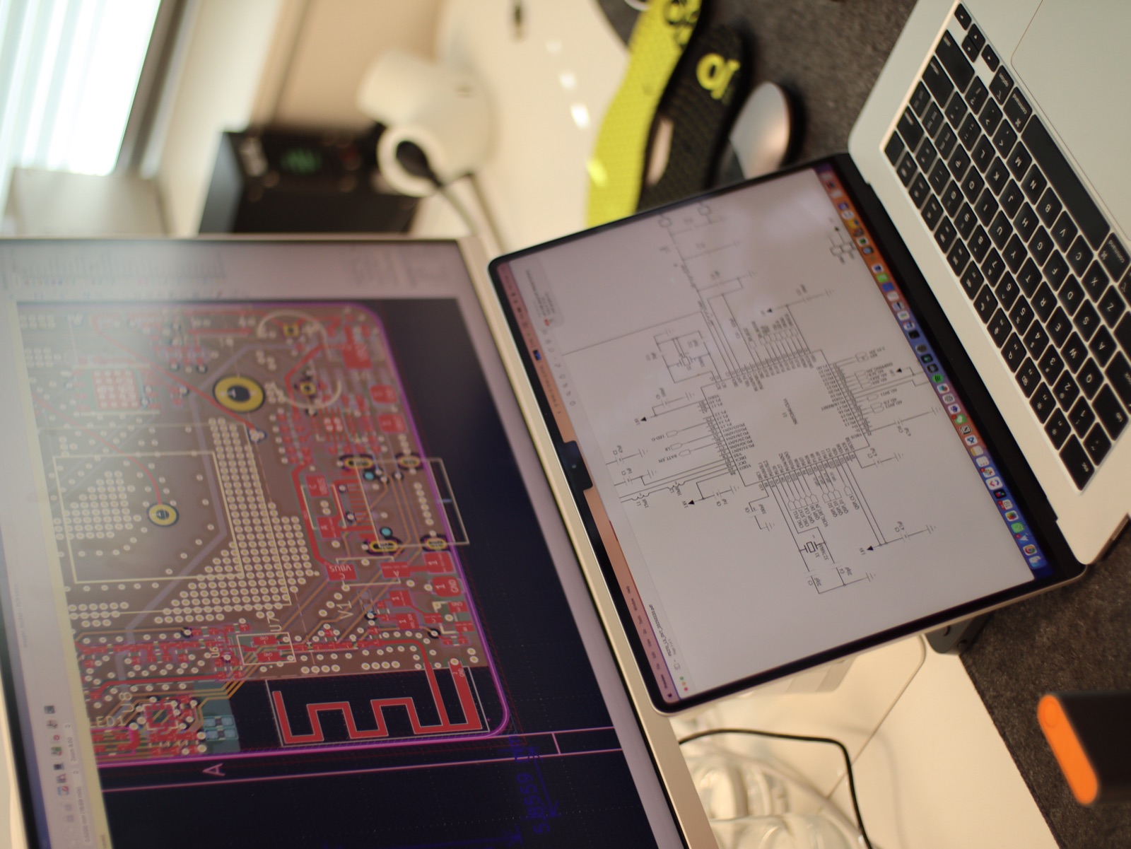
Getting a circuit board made starts with the design, and that is where you decide whether the product will be affordable to build later. We take your concept — a napkin sketch, a block diagram, a half-finished schematic — and turn it into a manufacturable, certifiable board. That applies to plain industrial electronics just as much as to wireless products.
Our specialism is the hard part: RF layouts, ultra-low-power designs, and multi-layer boards with integrated wireless modules. But most of our work is straightforward printed circuit board design — power, control, sensor read-out, connectors in the right place, and a layout your assembly partner will not trip over.
What We Design
RF & Antenna Layout
Bluetooth, Wi-Fi, LoRa, LTE-M, NB-IoT, GNSS/GPS
Low-Power Design
Ultra-low standby current, sleep modes, years-long battery operation
Sensor Integration
IMUs, environmental, proximity, optical, capacitive, custom interfaces
Edge Computing
nRF52/53, ESP32, STM32, i.MX RT, application-class SoCs
Also when there is no radio in it
Not every project is an IoT product. A large share of our hardware development is classic work: a drive that needs controlling, a measurement board that has to stay accurate, or an existing board that needs a redesign because a component went end-of-life. We are glad to take that on.
What you get on top is the rest of the house. PCB design, firmware, industrial design and cloud sit under one roof. Your enclosure engineer knows the board dimensions before layout begins, and your firmware developer sits next to the hardware designer. That removes exactly the handovers where most delay comes from.
We have designed boards for asset tracking, environmental monitoring, smart sports equipment, energy management and solar-powered remote sensing — and for projects with nothing connected at all.
Our PCB Design Process
Requirements & architecture review
Before opening a schematic tool, we align on power budget, target BOM cost, certification requirements, and mechanical constraints. Early decisions here prevent expensive respins later.
Schematic capture
Full schematic design in collaboration with you, selecting components through our global supply chain network (Mouser, DigiKey, LCSC). Optimised for performance and availability.
PCB layout
Component placement through routing, copper pours, and design rule checks. RF layouts receive particular attention: impedance-matched traces, antenna keep-out zones, and shielding strategies built in from the start.
Design for Manufacture (DFM) review
DFM analysis to catch pad issues, clearance violations, and assembly constraints. Our presence in Shenzhen means we know exactly what factories can handle.
Prototype & iteration
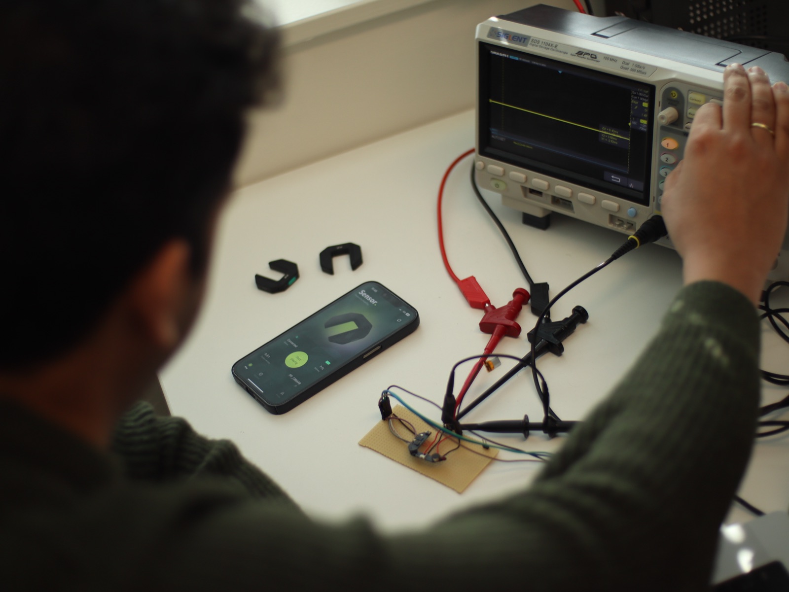
Prototype PCB production, bring-up, debugging, and design iterations through to a verified, stable design ready for volume production.
A PCB design brief you can quote and test
A useful brief connects the circuit to the product: what it measures or controls, where it fits, how it is powered and how many units you expect to build. We also design standalone electronics without a radio or cloud connection.
Agree the handover
Define the schematic, board layout, bill of materials and manufacturing files in the scope. Include assembly, firmware, test results and source files explicitly when you need them; a board layout alone does not cover all of these.
Budget for the engineering and the boards
Design effort depends on circuit complexity, space, power, interfaces and verification. Prototype fabrication and assembly are separate cost items. Agree how many revisions and which tests the estimate covers.
Bring the constraints
Share enclosure dimensions, connectors, supply voltage, target quantity and any existing drawings or prototype. Identify the hardest requirement early, such as a noisy sensor signal or a tight battery budget.
Plan how to accept the design
Set measurable checks before layout: voltage rails, current consumption, input accuracy and interface behaviour. Decide which evidence is needed before ordering a pilot batch.
Frequently asked questions
Do you design boards that are not IoT products?
Yes. Wireless and low-power work is our specialism, but a large share of our hardware development is ordinary industrial electronics: motor control, measurement and sensor boards, power supplies, and redesigns of existing boards whose components went end-of-life. If it is a circuit board, we can design it.
What kind of PCBs does Insyght design?
Multi-layer, high-density, and RF boards for connected products, from low-power sensor nodes to BLE, Wi-Fi and cellular devices and mixed-signal designs. Every schematic is delivered DFM-ready for smooth manufacturing.
Which wireless chips and microcontrollers do you work with?
We specialise in Nordic nRF52 and nRF53, ESP32, and ARM Cortex-M, and regularly design around BLE, Wi-Fi, LTE-M/NB-IoT, and LoRa.
Do you handle RF and antenna design?
Yes. We do impedance-controlled RF layout, antenna matching and tuning, and a pre-compliance review so the board is far more likely to pass certification on the first attempt.
Can you design for low power and battery operation?
Low-power design is a core specialty. We optimise sleep-current budgets, power sequencing, and battery and charging topologies to reach long battery life.
Do you also build the firmware and enclosure?
Yes. PCB design sits inside our full stack, so the same team can deliver firmware, industrial design, certification, and manufacturing, with no coordination between separate vendors.
We needed a way to get data from solar systems in off grid villages into our cloud. Not exactly a friendly environment to design for. Power is unreliable, conditions are tough, connectivity is limited at best. Insyght moved fast and delivered a solution that just works, with solid Bluetooth connectivity and no unnecessary complexity.

Explore More Services

Ready to Start Your PCB Design Project?
Building a product and need a board designed, or an existing one reworked? Let’s talk.
'%3e%3cpath%20d='M0.512578%2012.7977C0.512016%2014.8142%201.04302%2016.7831%202.0527%2018.5185L0.416016%2024.448L6.53152%2022.857C8.22299%2023.7706%2010.1181%2024.2494%2012.044%2024.2495H12.0491C18.4067%2024.2495%2023.582%2019.1162%2023.5847%2012.8067C23.586%209.74933%2022.3871%206.87435%2020.2089%204.71138C18.0311%202.54858%2015.1347%201.35686%2012.0486%201.35547C5.6902%201.35547%200.515297%206.48849%200.512672%2012.7977'%20fill='url(%23paint0_linear_1455_10349)'/%3e%3cpath%20d='M0.100313%2012.7941C0.0996563%2014.8831%200.649687%2016.9224%201.69537%2018.72L0%2024.8621L6.33478%2023.214C8.08022%2024.1582%2010.0454%2024.6561%2012.0451%2024.6568H12.0502C18.636%2024.6568%2023.9972%2019.3389%2024%2012.8035C24.0011%209.63629%2022.7591%206.65796%2020.5031%204.4175C18.2468%202.17731%2015.2468%200.942709%2012.0502%200.941406C5.46337%200.941406%200.102938%206.25862%200.100313%2012.7941ZM3.87291%2018.4104L3.63637%2018.0379C2.64206%2016.4691%202.11725%2014.6563%202.118%2012.7948C2.12006%207.36271%206.57544%202.94327%2012.054%202.94327C14.7071%202.94438%2017.2005%203.97062%2019.0759%205.83257C20.9512%207.69471%2021.9831%2010.1701%2021.9824%2012.8028C21.98%2018.2349%2017.5245%2022.6549%2012.0502%2022.6549H12.0463C10.2638%2022.654%208.51569%2022.179%206.99113%2021.2814L6.62831%2021.0679L2.86912%2022.0459L3.87291%2018.4104Z'%20fill='url(%23paint1_linear_1455_10349)'/%3e%3cpath%20d='M9.06383%207.83911C8.84014%207.34581%208.60473%207.33586%208.39202%207.32721C8.21783%207.31976%208.0187%207.32032%207.81977%207.32032C7.62064%207.32032%207.29711%207.39465%207.02364%207.69093C6.74989%207.98748%205.97852%208.70414%205.97852%2010.1617C5.97852%2011.6193%207.04848%2013.028%207.19764%2013.2259C7.34698%2013.4234%209.26323%2016.5103%2012.2981%2017.6978C14.8204%2018.6847%2015.3336%2018.4884%2015.881%2018.4389C16.4285%2018.3896%2017.6477%2017.7225%2017.8964%2017.0306C18.1453%2016.3389%2018.1453%2015.746%2018.0707%2015.6221C17.996%2015.4986%2017.7969%2015.4245%2017.4983%2015.2764C17.1997%2015.1283%2015.7317%2014.4115%2015.458%2014.3126C15.1843%2014.2138%2014.9853%2014.1645%2014.7861%2014.4612C14.587%2014.7573%2014.0152%2015.4245%2013.841%2015.6221C13.6669%2015.8201%2013.4926%2015.8448%2013.1941%2015.6966C12.8953%2015.5479%2011.9337%2015.2355%2010.7929%2014.2263C9.90523%2013.441%209.30598%2012.4712%209.1318%2012.1746C8.95761%2011.8784%209.11314%2011.7178%209.26286%2011.5702C9.39702%2011.4374%209.56155%2011.2242%209.71098%2011.0513C9.85986%2010.8783%209.90955%2010.7548%2010.0091%2010.5573C10.1088%2010.3595%2010.0589%2010.1865%209.98436%2010.0383C9.90955%209.89009%209.32933%208.42488%209.06383%207.83911Z'%20fill='white'/%3e%3c/g%3e%3cdefs%3e%3clinearGradient%20id='paint0_linear_1455_10349'%20x1='1158.85'%20y1='2310.61'%20x2='1158.85'%20y2='1.35547'%20gradientUnits='userSpaceOnUse'%3e%3cstop%20stop-color='%231FAF38'/%3e%3cstop%20offset='1'%20stop-color='%2360D669'/%3e%3c/linearGradient%3e%3clinearGradient%20id='paint1_linear_1455_10349'%20x1='1200'%20y1='2393.01'%20x2='1200'%20y2='0.941406'%20gradientUnits='userSpaceOnUse'%3e%3cstop%20stop-color='%23F9F9F9'/%3e%3cstop%20offset='1'%20stop-color='white'/%3e%3c/linearGradient%3e%3cclipPath%20id='clip0_1455_10349'%3e%3crect%20width='24'%20height='24'%20fill='white'%20transform='translate(0%200.941406)'/%3e%3c/clipPath%3e%3c/defs%3e%3c/svg%3e)